
Samsung breaks ground on HBM packaging plant, a year ahead of schedule
Samsung Electronics broke ground on November 12 on a high-bandwidth memory packaging plant at its Onyang campus, with operations scheduled for June 2028 — a year earlier than initially planned — and President Lee Jae Myung said about ₩40 trillion ($30 billion) of additional equipment investment would follow. The plant is the first of five HBM lines in a wider programme — ₩6 trillion ($4.48 billion) for construction, with the equipment investment to follow.
📊 Scorecard: our Bullish call on $005930.KS is scored from ₩208,000, the last close before it ran. Its first result comes after the next close.
The News
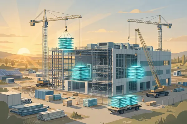
Samsung Electronics broke ground on November 12 on a high-bandwidth memory chip packaging plant at its Onyang campus in Asan, South Korea — Onyang Line 5, a three-storey plant of about 31,000 square metres set to produce seventh-generation HBM4E chips — as the first of five HBM lines in a wider programme, with ₩6 trillion ($4.48 billion) earmarked for construction across the lines. Operations are scheduled for June 2028, a year earlier than initially planned.
President Lee Jae Myung said the plant would be followed by about ₩40 trillion ($30 billion) of additional investment in advanced equipment. The plant sits inside a wider ₩144 trillion Samsung Group investment in the Chungcheong region, according to Dealroom, and SK Group has pledged $142.5 billion for the same region, including SK hynix NAND and packaging facilities — the two groups are building against each other in the same corridor.
The timing is the story. Packaging — stacking and sealing memory chips into the finished component — is the bottleneck of HBM production, and Samsung says demand for AI server memory is growing explosively, driven by Nvidia's AI chips and now Google's TPUs. Samsung is currently second to SK hynix in HBM, and bringing the plant forward by a year is its clearest statement yet that it does not intend to stay there.
Samsung is pouring concrete a year early — the HBM race is now a building race.
Why It Matters
Packaging is the bottleneck, and Samsung is attacking it. You can make all the memory chips in the world, but if you cannot stack and seal them into finished HBM fast enough, they never ship — and Samsung says demand for AI server memory is growing explosively, driven by Nvidia's AI chips and now Google's TPUs. A plant brought forward by a year is Samsung buying its way out of that bottleneck.
The scale of the regional build-out is the second signal. ₩144 trillion from Samsung Group and $142.5 billion pledged by SK Group in the same Chungcheong corridor is not two companies expanding — it is a national capacity race, with the president on stage promising follow-on investment. When governments and conglomerates both pour money into the same corridor, capacity stops being the constraint and market share becomes the contest.
The read-through for SK hynix is the honest counterweight. Samsung's plant does not shrink SK hynix's current lead — it raises the stakes. But for Samsung, the groundbreaking is the first concrete proof that its HBM catch-up is a building programme, not a press release, and the market's memory names trade on exactly that kind of proof.
The regional numbers show how big this build-out really is. Of Samsung Group's Chungcheong investment — ₩144 trillion on Dealroom's account, with Samsung Electronics at ₩60 trillion and Samsung Display at ₩67 trillion (Korean outlets report the group total as 144 trillion won: 60 trillion from Samsung Electronics and 67 trillion from Samsung Display), with SDI and Electro-Mechanics making up the rest — and SK Group's $142.5 billion pledge for the same region includes SK hynix NAND and packaging facilities. Two conglomerates spending a quarter of a trillion dollars in one corridor is a bet that HBM demand will be there for years, not quarters.
Analyst's Take
Our call is Bullish. A groundbreaking a year ahead of schedule, with ₩40 trillion of follow-on equipment investment promised by the president, is not a routine expansion — it is a capacity race being fought with concrete. Samsung is telling the market it will have the packaging capacity to meet HBM demand when it arrives, and the June 2028 start date puts it in the fight for the next generation of AI chips.
What to watch: whether Samsung can convert the plant into actual HBM market share against SK hynix, and whether Google's TPU expansion — which Samsung is pursuing through its Broadcom partnership, with no confirmed HBM orders yet — gives it a second big customer to fill the new capacity. The plant is real; the orders to fill it are the next test.
Are you bullish or bearish on this story?
By The Numbers
FAQ
What is HBM?
HBM stands for high-bandwidth memory — a specialised memory chip stacked in layers and placed next to an AI processor, feeding it data far faster than ordinary memory. Nvidia's AI chips and Google's TPUs both use HBM, which is why it is the most fought-over part of the memory market.
What is chip packaging?
Packaging is the step where finished memory chips are stacked, bonded and sealed into the final component that goes into an AI system. It is the bottleneck of HBM production: you can make the memory, but if you cannot package it fast enough, it never ships. Samsung's new plant is a packaging plant, not a chip-making fab.
Why is Samsung building a year early?
Operations are scheduled for June 2028, a year earlier than initially planned — a signal of urgency. Samsung is racing SK hynix, which currently leads the HBM market, and Samsung says demand for AI server memory is growing explosively. Bringing the plant forward is Samsung's way of saying it does not intend to stay second.
What is HBM4E?
HBM4E is the seventh generation of high-bandwidth memory — the next step after HBM4, with more memory stacked in each package and faster data transfer. The new Onyang Line 5 plant, a three-storey building of about 31,000 square metres, is set to produce it.
Who is SK hynix in this race?
SK hynix is Samsung's great rival in memory and the current HBM leader, with about 50% of global HBM revenue in the second quarter of 2026, ahead of Samsung at 33% (Counterpoint Research). Its parent, SK Group, has pledged $142.5 billion for the same Chungcheong region, including SK hynix NAND and packaging facilities — the two groups are building against each other in the same corridor.
👁
Source: WIXX (Reuters)